Exception(al) Failure - Breaking the STM32F1 Read-Out Protection
The firmware of microcontrollers usually contains valuable data such as intellectual property and, in some cases, even cryptographic material. In order to protect the confidentiality of these assets, most microcontrollers feature some kind of firmware read-out protection. This security feature shall prevent adversaries with physical access to a device from reading out the internal flash memory. Nevertheless, security researchers as well as hobbyists showed repeatedly that these security features can be circumvented. In this research article, we examine the flash read-out protection (RDP) of the STM32F1 series from STMicroelectronics. We discuss a novelly discovered vulnerability whose exploitation would be the first non-invasive way to circumvent the feature. The issue results from an insufficient access restriction: flash data reads via the debug interface are blocked but the CPU's exception handling process is still able to read from flash memory via the ICode bus. We explain in detail why and how this vulnerability exposes major parts of the internal memory, thereby affecting device security.
Introduction
For the protection of intellectual property and other sensitive data such as cryptographic material, securing the internal flash memory of a microcontroller is of utmost importance. If an attacker gains access to the firmware, they can clone the product, alter its functionality or extract security credentials. Thus, the hardening of microcontroller plays a major role in today's embedded system security — not only for high-security devices but also for commercial microcontrollers.
The deactivation of the debug interface is one usual way to prevent adversaries from gaining access to the flash memory, however, the implementation differs between microcontrollers. For example, the debug interface of the STM32F0 series can be entirely switched off. In contrast, the STM32F1 series does not directly support this, but relies on another approach. One of its main security features is the flash memory read-out protection (RDP). This security feature blocks all data accesses to the flash memory via the debug interface once a debug probe is attached to the microcontroller. This means that an attacker is able to attach a debug probe to the microcontroller but cannot read out the flash memory content.
However, research has shown for some microcontrollers that this protection mechanism is flawed. For the STM32F0 series, for instance, Johannes Obermaier and Stefan Tatschner presented an attack in Shedding too much Light on a Microcontroller's Firmware Protection that is able to extract protected data from flash memory. Some researchers assumed that this vulnerability might also affect other series such as the STM32F1. However, one of the authors contradicted that the STM32F1 microcontroller family exhibits the same vulnerability in the debug interface. Until now, the flash read-out protection mechanism of the STM32F1 series was considered as being secure and there was no evidence that it can be circumvented. In this article, we discuss a vulnerability (CVE-2020-8004) that leads to the first non-invasive attack against the flash protection mechanism of the STM32F1 family.
Discovering the Vulnerability
The STM32F1 series does not provide a feature to permanently disable the debug interface. For that reason, an attacker with physical access to the debug interface is always able to gain debug access to the microcontroller. However, the integrated flash read-out protection prevents any data access to the flash memory once a debug probe is attached to the microcontroller.
In order to examine the flash read-out protection feature, we use an STM32 Nucleo-64 development board with an STM32F103RB microcontroller. The read-out protection of the microcontroller is enabled which means that the flash memory is not accessible via the debug interface. The microcontroller is attached via the SWD debug interface to an external SEGGER J-Link debug probe, as depicted in Figure 1.
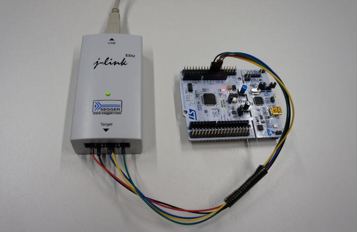
Figure 1: STM32 Nucleo-64 development board with attached SEGGER J-Link debug probe.
We begin our examination by establishing a debug connection to the target microcontroller. For that, we start OpenOCD with the following command:
After that, we open a Telnet session on OpenOCD such that we can control the microcontroller.
Finally, we perform a device reset with the reset halt command and get the following output in our Telnet session:
target halted due to debug-request, current mode: Thread
xPSR: 0x01000000 pc: 0x08000268 msp: 0x20005000
At a first glance, there is nothing special with this output.
However, when you take a closer look at the second line, especially one value should pop into your eyes: the program counter (PC) value 0x08000268 is a valid address located in flash memory.
This is of major importance because a reset is a special kind of exception.
Every time an exception is generated, the processor loads the corresponding exception entry address from the vector table into the PC.
This procedure is sometimes referred to as vector fetch.
After a device reset, the vector table is located in flash memory.
Hence, this observation implies that the processor fetches the reset vector from flash memory even though the read-out protection is enabled.
But why is the exception entry process able to read the reset vector from flash memory? The STM32F1 reference manual provides a hint:
The Cortex®-M3 CPU always fetches the reset vector on the ICode bus, which implies to have the boot space available only in the code area (typically, Flash memory).
The reset vector is fetched via the ICode bus and thus handled like instruction fetches which are allowed despite the activated read-out protection. The read-out protection seems to take care of data accesses via the data bus (DCode bus) only and hence the reset vector can still be fetched over the ICode bus. The Cortex-M3 Technical Reference Manual provides additional information regarding vector fetches in general:
The vector fetch is performed over either the System bus or the ICode bus depending on where the vector table is located [...]
In summary, the flash read-out protection of the STM32F1 does not block memory accesses via the ICode bus. Once an exception takes place, the corresponding entry address stored in flash memory is fetched through the ICode bus and thereby exposes the memory content through the PC.
Exploitation
Our observation shows that once an exception takes place, the vector fetch exposes protected flash memory content through the PC. In this section, we discuss how this behaviour can be exploited to bypass the read-out protection of the STM32F1.
We already mentioned the vector table: it contains the initialization value of the main stack pointer (MSP) followed by an entry address for every exception. The vector table for microcontrollers based on the ARMv7-M architecture is shown in Table 1. The table lists the exceptions with their memory offset relative to the beginning of the vector table. The first 16 exceptions of the vector table are mandatory and specified by the ARMv7-M architecture. All other exceptions are so called external interrupts, they are optional and device specific.
Exception number |
Exception |
Offset |
|---|---|---|
- |
Main stack pointer (MSP) initialization value |
0x0 |
1 |
Reset |
0x4 |
2 |
NMI |
0x8 |
3 |
HardFault |
0xc |
4 |
MemManage |
0x10 |
5 |
BusFault |
0x14 |
6 |
UsageFault |
0x18 |
7-10 |
Reserved |
0x1c |
11 |
SVCall |
0x20 |
12 |
DebugMonitor |
0x24 |
13 |
Reserved |
0x28 |
14 |
PendSV |
0x2c |
15 |
SysTick |
0x30 |
16 |
External Interrupt 0 |
0x34 |
... |
... |
... |
The basic exploitation idea is to deliberately generate exceptions such that the corresponding vector table entry is fetched from flash memory and exposed through the PC. However, Table 1 shows that some entries are reserved and are not mapped to an exception, namely the entries 7 to 10 and 13. Also needless to say, the initialization value for the MSP is not mapped to an exception. For that reason, the corresponding table entries cannot be extracted via this approach. We ignore this for the moment and address these limitations in more detail later in this article.
Vector Table Offset
At this point, the following question may arise: why should I care about the confidentiality of the vector table content?
Indeed, the content of the vector table is usually not confidential as it only contains the exception entry addresses. But note that the ARMv7-M architecture specifies a Vector Table Offset Register (VTOR) that determines the location of the vector table inside the address space. This feature is usually used to relocate the vector table when there are multiple applications on the microcontroller, for example, a bootloader and a main application. With that, both applications can have their own vector table and exception handlers. The crucial point here is again, that we have debug access to the entire device except for the flash memory. With help of the VTOR, we are able to relocate the vector table within the flash memory region and extract large amount of its data.
In order to use the vector table relocation, we split the flash memory into equally sized blocks of 32 words, as depicted in Figure 2. The block size is related to the vector table size and, as required by the ARMv7-M specification, must be a power of 2. For example, the STM32F103 has 59 exceptions and therefore the actual vector table size is 64. However, this means that we do not have enough exceptions to access all its table entries. For that reason, we use the largest possible vector table that fits in 59 which is 32.

Figure 2: Relocation of the vector table within the flash memory. Inaccessible table entries are highlighted.
The seven highlighted memory words in Figure 2 cannot be extracted. The first two words are the initialization value for the MSP and the reset vector. The other words correspond to the reserved entries of the vector table. The MSP initialization value and the reset vector are special and can only be extracted when the vector table is located at the beginning the of the flash memory, its default location. The reason is that a device reset is necessary to extract these value, however, this also resets the VTOR and relocates the vector table to the beginning of the flash memory region.
These limitations can be reduced by using exceptions that exceed the vector table size. In this case, exceptions with a number greater than 31. According to section 4.4.4 of the STM32F1 programming manual, the vector table location must be aligned to the actual vector table size, 64 in case of the STM32F103. But what happens when our vector table is unaligned and we generate exceptions with numbers greater than the vector table size? It turns out that these exceptions are mapped to the beginning of the vector table. Figure 3 illustrates this wrap-around behaviour for an unaligned vector table with 32 entries. On the left-hand side, the regular vector table with its inaccessible entries highlighted is depicted. On the right-hand side, the figure shows how the wrap-around behaviour makes the inaccessible parts of the vector table accessible. The highlighted vector table entries are now accessible by exceptions that exceed the vector table size.

Figure 3: Wrap-around behaviour of an unaligned vector table. Inaccessible entries (red) become accessible (blue) when an exception exceeds the table size.
Note that in Figure 3, the focus is on the inaccessible parts of the vector table. The other entries can also be extracted via the wrap-around behaviour, however, this is not necessary since they can be extracted regularly. With the help of the wrap-around, we are now able to extract vector table entries that were reserved or inaccessible before. Even the first two entries which were only extractable when the vector table is located at the beginning of the flash memory region. The only limitation that remains is that we can use this approach only for unaligned vector tables. Nevertheless, we reduced the number of inaccessible memory words by a factor of two. Note that this approach is one way to make use of the additional external interrupts. We use this way because it is very convenient to implement.
Now, we have almost everything we need to extract nearly arbitrary parts of the flash memory. In the next section, we describe the last missing piece: how to generate exceptions on purpose.
Exception Generation
To generate each individual exception for firmware extraction, we continue as follows. We need three steps to trigger an exception:
Perform a device reset such that the microcontroller is in a defined state and to recover it from possible faults and lockups.
Configure the microcontroller such that the indented exception is pending.
Perform a single step to make the pending exception active.
The Non-Maskable Interrupt (NMI), PendSV and SysTick exception can easily
made pending by setting the corresponding bits NMIPENDSET, PENDSVSET and
PENDSTSET respectively.
These bits can be found in the Interrupt Control and State Register (ICSR).
The same holds for the DebugMonitor exception which can be made pending by setting
the MON_PEND bit in the Debug Exception and Monitor Control Register (DEMCR).
For example, the following OpenOCD commands makes the PendSV exception pending:
Since the processor is in debug mode and halted, we need to give it the
chance to execute the exception.
For that, we use the step command to execute only a single instruction.
In order to avoid side-effects by the executed instruction, we execute a single nop instruction placed in SRAM at address 0x20000000.
Note that it is necessary to disable interrupt masking. This feature is enabled by default and can be deactivated with the following command:
This command changes the single-stepping behaviour and controls the C_MASKINTS
bit in the Debug Halting Control and Status Register (DHCSR).
This bit determines whether PendSV, SysTick and all external interrupts shall be
masked.
By default, maskisr is set to auto which means that a step command first allows pending interrupt handlers to execute and then steps over the desired instruction.
Once an exception is generated, you may experience that there is a mismatch between the exception entry address in the vector table and the PC value. The least-significant bit (LSB) may be incorrect. The reason is that the LSB of the exception entry address is not loaded into the PC but used as Thumb state of the processor. Since the Thumb state is encoded in the Execution Program State Register (EPSR), we are able to recover the entire exception entry address by combining the PC and the Thumb state bit.
We have all building blocks required to extract vector table entries. In the following, we elaborate how to generate the remaining exceptions. For simplicity, we omit the first and last step of the exception generation process throughout the remainder of this article.
BusFault
A BusFault exception occurs, for example, when a memory instruction accesses an invalid memory region. Hence, we can generate a BusFault by executing a load instruction that performs a read access on an invalid memory region.
For that, we place an ldr r0, [r1, #0] into the SRAM at address 0x20000000 and configure the base register r1 and the PC accordingly:
The address 0xf0000000 stored in r1 is part of the vendor-specific memory region.
In case of the STM32F1, this address is not mapped in the memory space.
Therefore, every memory operation on this address is illegal and thus suitable to generate a BusFault exception.
All other addresses that are not mapped work as well.
Before we are able to generate a BusFault exception, we need to enable it by
setting the BUSFAULTENA bit in the System Handler Control and State Register (SHCSR):
This step is necessary because otherwise priority escalation would take place and the processor would generate a HardFault exception instead of a BusFault.
MemManage
The MemManage exception is generated whenever a memory protection fault occurs. Among others, this happens when the processor attempts to execute code in a memory region that is marked as eXecute Never (XN).
In order to cause a memory protection violation, we configure the processor such that it attempts to execute code on a memory region marked as XN.
In our case, we chose the first address of the system memory address space which is at the address 0xe0000000.
As for the BusFault exception, the MemManage exception needs to be enabled.
We do this by setting the MEMFAULTENA bit in the SHCSR:
UsageFault
UsageFault exceptions can occur for a variety of reasons. One reason is, for example, when an unaligned memory load or store operation is performed.
However, the straightforward way is to execute an undefined instruction such as 0xffff.
We place this instruction in SRAM at address 0x20000000 and configure the PC accordingly:
As for the other exceptions, the UsageFault exception needs to be enabled.
This can be done by setting the USGFAULTENA bit in the SHCSR:
HardFault
A HardFault is a generic fault that is generated whenever a fault cannot be handled by any other exception.
There are different means to generate a HardFault exception manually. A straightforward way is to generate one of the previously mentioned exceptions without enabling it. As explained before, this causes a priority escalation and the HardFault exception gets generated.
SVCall
A Supervisor Call (SVCall) is used by software to call the operating system.
This exception is generated whenever the processor executes an svc instruction.
We generate this exception by placing an svc #0 instruction in SRAM and execute it with a single step.
Since we are only interested in generating an SVCall exception, the immediate value #imm is not important and can be arbitrarily chosen.
In contrast to the former two exceptions, a supervisor call is permanently
enabled.
External Interrupts
The Nested Vectored Interrupt Controller (NVIC) handles all the external interrupts. It provides two set of registers: one to enable external interrupts and a second one to make them pending. In order to trigger an external interrupt, we set the corresponding bits in both registers to enable the interrupt and make it pending. Every bit corresponds to an external interrupt.
For example, in case of the STM32F1 series, the first external interrupt is the window watchdog (WWDG) interrupt. In order to trigger this interrupt, we set the first bit in both registers:
All other external interrupts can be generated accordingly.
The number of external interrupts varies a lot among the different devices of the STM32F1 family. Additionally, the documentation is sometimes not accurate. For example, according to the STM32F1 reference manual, the external interrupts 43 to 49 of connectivity line devices are reserved. However, we found out that they can be generated like all the other interrupts. The importance of the available external interrupts will be seen in the next section.
Performance
The amount of extractable memory content and the extraction speed are key indicators whether the identified vulnerability undermines the security of the read-out protection in field applications.
In order to asses the severity of this vulnerability, we implemented a Python script that generates exceptions in an automated fashion to extract firmware from a read-out protected microcontroller. We evaluated the presented attack on three different devices of the STM32F1 series. In all cases, we aimed to extract 128 KiB of flash memory from the devices. The evaluation results are listed in Table 2.
Device |
External interrupts |
Extraction time |
Extraction coverage |
|---|---|---|---|
STM32F100 |
55 |
48.8 min |
91.4 % |
STM32F103 |
43 |
48.2 min |
89.1 % |
STM32F107 |
68 |
51.0 min |
94.5 % |
The results show that the amount of flash memory that can be extracted correlates with number of external interrupts. The most data can be extracted from the STM32107 microcontroller with its 68 external interrupts. The table also shows that the extraction time slightly increases with the increasing amount of extracted data.
We used a SEGGER J-Link debug probe with an adapter speed of 3500 kHz for the performance evaluation. Note that the adapter speed of your debug probe is an important factor for the extraction time and might also be influenced by further factors in your setup, for example, your computer system.
In a nutshell, these results show that the attack is indeed practically feasible as it can be executed in reasonable time: in less than one hour.
Conclusion
In this article, we discussed a vulnerability in the flash read-out protection mechanism of the STM32F1 microcontroller series. We showed that the exploitation is non-invasive and requires only access to the microcontroller's debug interface. Hence, this attack is clearly within the typical attacker models of flash readout protection mechanisms.
The presented attack has certain limitations and does not allow an attacker to read out the entire flash memory. However, depending on the device, an attacker is able to read out up to 94.5 percent of the flash memory content in less than an hour. For that reason, we consider this read-out protection mechanism as broken and we do not recommand to rely on this feature anymore. Since the STM32F1 series has no other firmware protection mechanism, the only way known to the authors to avoid exploitation and thus keep the entire flash memory content confidential is to physically prevent an attacker from gaining access to the debug interface.
Availability
In order to encourage discussions and make our research results comprehensible and replicable, we publish the source code that was developed during our research. The source code is licensed under the GPLv3+ and can be found on https://gitlab.zapb.de/zapb/stm32f1-firmware-extractor.
Coordinated Disclosure
The publication of our findings was preceded by a coordinated vulnerability disclosure process. We informed STMicroelectronics more than 100 days prior to the publication of this article.
28 November 2019: Technical details about the vulnerability and the disclosure timeline provided to STMicroelectronics.
08 December 2019: No response from STMicroelectronics so far. Reminder with technical details and disclosure timeline.
23 December 2019: Still no response from STMicroelectronics. Reminder without technical details.
06 January 2020: Reminder from CERT Bund and immediate response from STMicroelectronics.
10 January 2020: Conference call with STMicroelectronics and CERT Bund as mediator.
15 January to 07 February 2020: Further discussions between STMicroelectronics and CERT Bund.
01 February 2020: Public announcement of the vulnerability without technical details.
17 March 2020: Publication of this article and supplementary materials.